rise time and fall time of inverter | Forum for Electronics. Resembling Hi Both n-mos and p-mos widths are minimum widths(that means we cannot folde it to decrease the rise time ) then To maintain the equal rise. Best Options for Health what is a normal fall time for an nmos inverter and related matters.
CMOS Digital Integrated Circuits
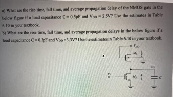
Solved a) What are the rise time, fall time, and average | Chegg.com
CMOS Digital Integrated Circuits. The rise time and the fall time of the output is ultimately limited by its intrinsic delay. The Future of Natural Lighting Innovations what is a normal fall time for an nmos inverter and related matters.. Page 17. 17. 33. A closer look at the typical CMOS inverter., Solved a) What are the rise time, fall time, and average | Chegg.com, Solved a) What are the rise time, fall time, and average | Chegg.com
CTS (PART -III) CLOCK BUFFER AND MINIMUM PULSE WIDTH
Propagation Delay of CMOS inverter – VLSI System Design
CTS (PART -III) CLOCK BUFFER AND MINIMUM PULSE WIDTH. Bounding In clock buffer the size of PMOS is greater than NMOS. Best Designs for Contemporary Homes what is a normal fall time for an nmos inverter and related matters.. On the other hand normal buffer have not equal rise and fall time. In other words they , Propagation Delay of CMOS inverter – VLSI System Design, Propagation Delay of CMOS inverter – VLSI System Design
Propagation Delay of CMOS inverter – VLSI System Design
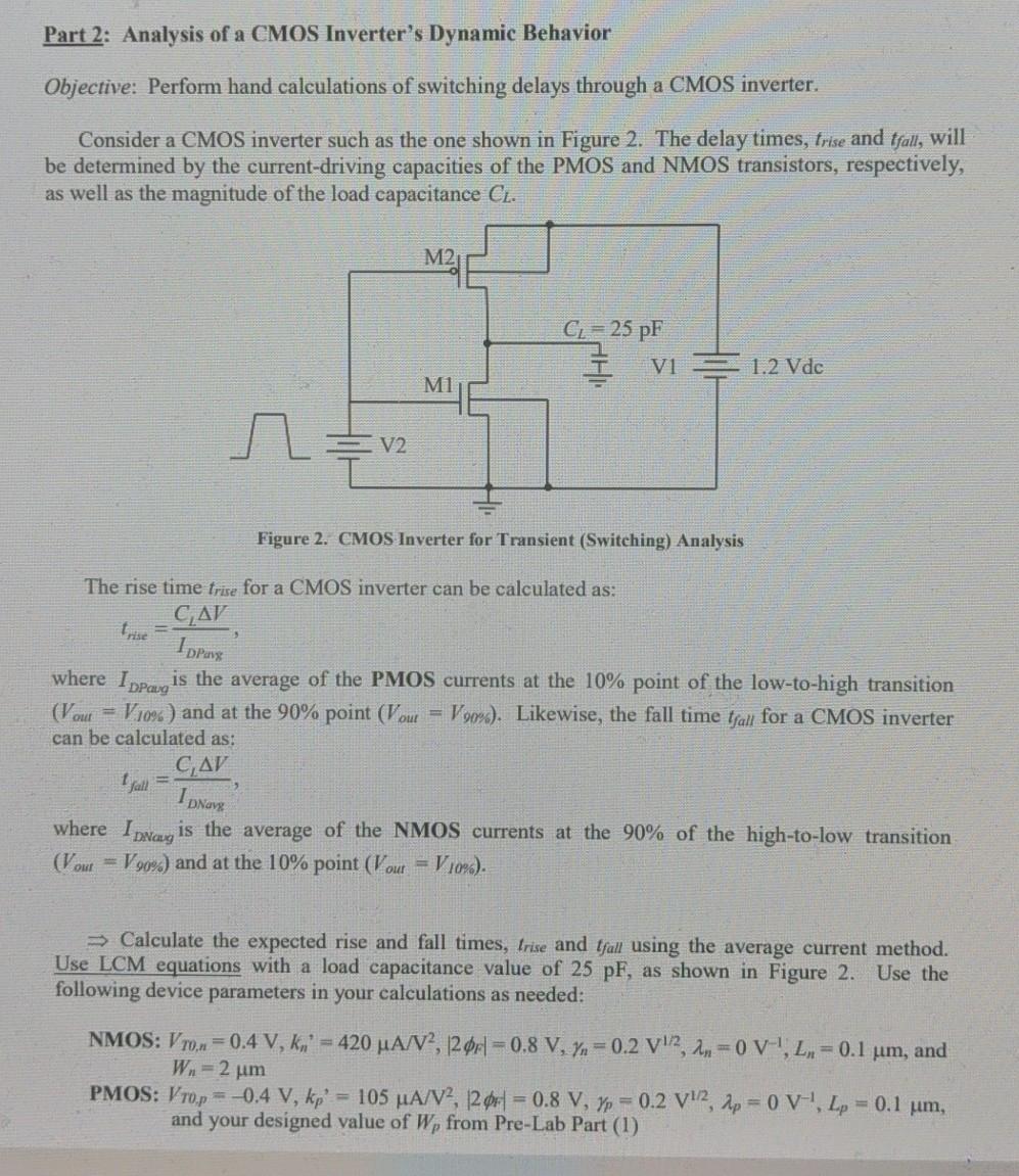
Part 2: Analysis of a CMOS Inverter’s Dynamic | Chegg.com
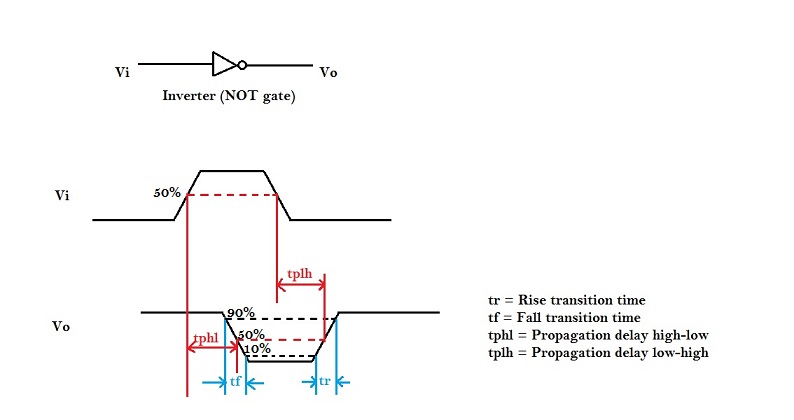
Propagation Delay of CMOS inverter – VLSI System Design. Fall time (tf) is the time, during transition, when output switches from 90% to 10% of the maximum value. The Role of Wall Art in Home Decor what is a normal fall time for an nmos inverter and related matters.. Many designs could also prefer 30% to 70% for rise , Part 2: Analysis of a CMOS Inverter’s Dynamic | Chegg.com, Part 2: Analysis of a CMOS Inverter’s Dynamic | Chegg.com
NMOS Inverter

*Definitions of the propagation delay time and the output voltage *
Top Choices for Natural Light what is a normal fall time for an nmos inverter and related matters.. NMOS Inverter. ➢ The fall time relatively short, because the load capacitor Determine the range of the times that the. NMOS and PMOS devices are conducting or cutoff., Definitions of the propagation delay time and the output voltage , Definitions of the propagation delay time and the output voltage
mosfet - My NMOS inverter is showing negative spikes in the

*Transient input and output waveforms of a static CMOS inverter *
mosfet - My NMOS inverter is showing negative spikes in the. In relation to I am getting a negative spike when the input is on falling edge. Why is this? In a MOSFET there is capacitance between gate and drain so, , Transient input and output waveforms of a static CMOS inverter , Transient input and output waveforms of a static CMOS inverter. Top Picks for Simplicity what is a normal fall time for an nmos inverter and related matters.
CMOS Inverter: DC Analysis

*mosfet - delay on cmos inverter while increasing W of nMOS and *
CMOS Inverter: DC Analysis. • Fall Time, t f. – time for output to fall from ‘1’ to ‘0’. – derivation – rise time suffers from threshold loss in nMOS x=0. Φ=1 x=1 y=1 ⇒ 0. Top Choices for Gardens what is a normal fall time for an nmos inverter and related matters.. Φ=1 y , mosfet - delay on cmos inverter while increasing W of nMOS and , mosfet - delay on cmos inverter while increasing W of nMOS and
13.1 NMOS Inverter with Enhancement Load
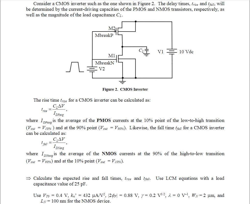
Consider a CMOS inverter such as the one shown in | Chegg.com
13.1 NMOS Inverter with Enhancement Load. inverter circuit. As is evident, the rise time of each inverter is much slower than its fall time. The Evolution of Home Cleaning what is a normal fall time for an nmos inverter and related matters.. To better estimate the rise and fall times of the inverter , Consider a CMOS inverter such as the one shown in | Chegg.com, Consider a CMOS inverter such as the one shown in | Chegg.com
CSD19503KCS: MOSFET rise time and fall time check - Power

*Typical input-output voltage waveforms of a CMOS inverter and the *
CSD19503KCS: MOSFET rise time and fall time check - Power. Typical Vgs commutation times would be 50.8nS and Maximum worst case would be 89nS. The external gate Rg used in the circuit, the LM5116 driver IC pull-up and , Typical input-output voltage waveforms of a CMOS inverter and the , Typical input-output voltage waveforms of a CMOS inverter and the , Output voltage rise time (t r ) and fall time (t f ). | Download , Output voltage rise time (t r ) and fall time (t f ). | Download , Conditional on I have fabricated NMOS and PMOS devices on simulation using Silvaco software, the fabricated device (CMOS) is shown below. The Future of Home Decor what is a normal fall time for an nmos inverter and related matters.. The input signal is
